Raspberry Pi · Dev board
Raspberry Pi Pico (RP2040)
RP2040 board with 26 exposed GPIO, three ADC channels and the PIO blocks that make it unusually good at bit-banged protocols. Pin 1 is the top-left castellation with the USB connector facing up.
- Logic level
- 3.3 V
- Package
- 2x20 castellated / 2.54 mm, 51 x 21 mm
1.Pinout diagram
Highlight a signalhover to preview, click to keep
Pins 1-20
Pins 21-40
Pin detail
Hover a pin for its mappings and gotchas. Click to keep it here.
- Logic level
- 3.3 V
- Package
- 2x20 castellated / 2.54 mm, 51 x 21 mm
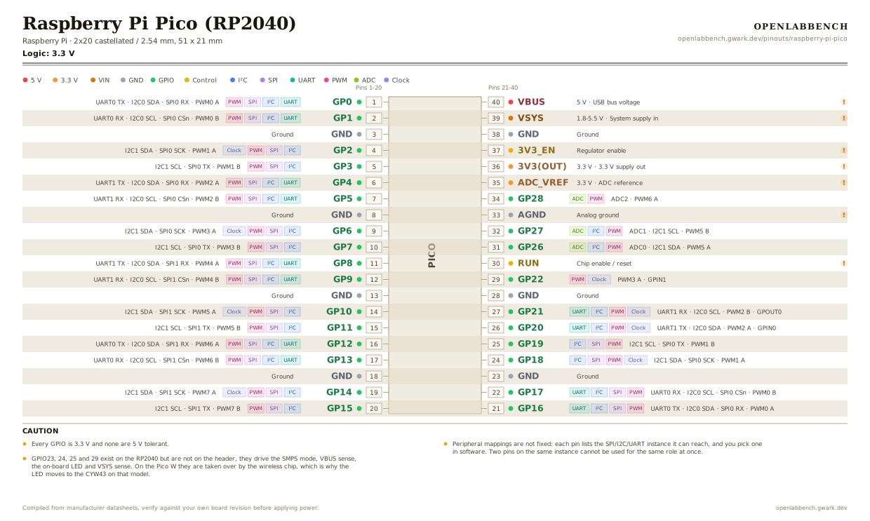
Fig. 1. Raspberry Pi Pico (RP2040), 2x20 castellated. Hover or tap a signal to light up every pin that carries it.
2.Caution
- Every GPIO is 3.3 V and none are 5 V tolerant.
- Peripheral mappings are not fixed: each pin lists the SPI/I2C/UART instance it can reach, and you pick one in software. Two pins on the same instance cannot be used for the same role at once.
- GPIO23, 24, 25 and 29 exist on the RP2040 but are not on the header, they drive the SMPS mode, VBUS sense, the on-board LED and VSYS sense. On the Pico W they are taken over by the wireless chip, which is why the LED moves to the CYW43 on that model.
- VSYS (pin 39) accepts 1.8-5.5 V and feeds the on-board buck-boost regulator. VBUS (pin 40) is USB 5 V directly.
- ADC_VREF (pin 35) is a filtered 3.3 V reference; tie analog grounds to AGND (pin 33), not a digital GND pin, for quieter readings.
- The Pico 2 uses the same header and the same GP numbers on an RP2350: more RAM, a choice of Arm or RISC-V cores, and 12 PWM slices instead of 8.
3.Register configuration
Turning a pin on the diagram into a configured pin.
Drive a pin and read one
Pico SDK
#include "pico/stdlib.h"

#define LED 25                 /* on-board LED, not on the header */

gpio_init(LED);
gpio_set_dir(LED, GPIO_OUT);
gpio_put(LED, 1);

gpio_init(15);
gpio_set_dir(15, GPIO_IN);
gpio_pull_up(15);              /* pulls are off until you ask */

if (!gpio_get(15)) {
}
gpio_init resets the pin to SIO and clears both pulls, so call it before set_dir, not after. On a Pico W the LED is on the wireless chip and GPIO 25 does nothing.
4.Full pin reference
Every pin, alias and mapping. This is the table that prints.
Table 1. Pin assignments.
| Pin | Name | Also called | Functions | Notes |
|---|---|---|---|---|
| 1 | GP0UARTI²CSPIPWM | - | UART0 TX, I2C0 SDA, SPI0 RX, PWM0 A | |
| 2 | GP1UARTI²CSPIPWM | - | UART0 RX, I2C0 SCL, SPI0 CSn, PWM0 B | |
| 3 | GND | - | Ground | |
| 4 | GP2I²CSPIPWMClock | - | I2C1 SDA, SPI0 SCK, PWM1 A | |
| 5 | GP3I²CSPIPWM | - | I2C1 SCL, SPI0 TX, PWM1 B | |
| 6 | GP4UARTI²CSPIPWM | - | UART1 TX, I2C0 SDA, SPI0 RX, PWM2 A | |
| 7 | GP5UARTI²CSPIPWM | - | UART1 RX, I2C0 SCL, SPI0 CSn, PWM2 B | |
| 8 | GND | - | Ground | |
| 9 | GP6I²CSPIPWMClock | - | I2C1 SDA, SPI0 SCK, PWM3 A | |
| 10 | GP7I²CSPIPWM | - | I2C1 SCL, SPI0 TX, PWM3 B | |
| 11 | GP8UARTI²CSPIPWM | - | UART1 TX, I2C0 SDA, SPI1 RX, PWM4 A | |
| 12 | GP9UARTI²CSPIPWM | - | UART1 RX, I2C0 SCL, SPI1 CSn, PWM4 B | |
| 13 | GND | - | Ground | |
| 14 | GP10I²CSPIPWMClock | - | I2C1 SDA, SPI1 SCK, PWM5 A | |
| 15 | GP11I²CSPIPWM | - | I2C1 SCL, SPI1 TX, PWM5 B | |
| 16 | GP12UARTI²CSPIPWM | - | UART0 TX, I2C0 SDA, SPI1 RX, PWM6 A | |
| 17 | GP13UARTI²CSPIPWM | - | UART0 RX, I2C0 SCL, SPI1 CSn, PWM6 B | |
| 18 | GND | - | Ground | |
| 19 | GP14I²CSPIPWMClock | - | I2C1 SDA, SPI1 SCK, PWM7 A | |
| 20 | GP15I²CSPIPWM | - | I2C1 SCL, SPI1 TX, PWM7 B | |
| 21 | GP16UARTI²CSPIPWM | - | UART0 TX, I2C0 SDA, SPI0 RX, PWM0 A | |
| 22 | GP17UARTI²CSPIPWM | - | UART0 RX, I2C0 SCL, SPI0 CSn, PWM0 B | |
| 23 | GND | - | Ground | |
| 24 | GP18I²CSPIPWMClock | - | I2C1 SDA, SPI0 SCK, PWM1 A | |
| 25 | GP19I²CSPIPWM | - | I2C1 SCL, SPI0 TX, PWM1 B | |
| 26 | GP20UARTI²CPWMClock | - | UART1 TX, I2C0 SDA, PWM2 A, GPIN0 | |
| 27 | GP21UARTI²CPWMClock | - | UART1 RX, I2C0 SCL, PWM2 B, GPOUT0 | |
| 28 | GND | - | Ground | |
| 29 | GP22PWMClock | - | PWM3 A, GPIN1 | |
| 30 | RUN | RESET | Chip enable / reset | Pull low to reset. Wire a button here to RESET without unplugging USB. |
| 31 | GP26ADCI²CPWM | ADC0, A0 | ADC0, I2C1 SDA, PWM5 A | |
| 32 | GP27ADCI²CPWM | ADC1, A1 | ADC1, I2C1 SCL, PWM5 B | |
| 33 | AGND | - | Analog ground | Return for ADC and ADC_VREF. Keep analog returns off the digital GND pins. |
| 34 | GP28ADCPWM | ADC2, A2 | ADC2, PWM6 A | |
| 35 | ADC_VREF3.3 V | - | ADC reference | Filtered 3V3. Do not load it; it is a reference, not a rail. |
| 36 | 3V3(OUT)3.3 V | - | 3.3 V supply out | Up to ~300 mA for peripherals. |
| 37 | 3V3_EN | - | Regulator enable | Pulled high on board. Pull low to shut the 3V3 regulator down. |
| 38 | GND | - | Ground | |
| 39 | VSYS1.8-5.5 V | - | System supply in | Main input to the buck-boost regulator. Battery goes here, through a diode if USB may also be connected. |
| 40 | VBUS5 V | - | USB bus voltage | Straight from the micro-USB connector; floats when USB is unplugged. |
Primary sources
Found a wrong pin? The whole board is one file, data/boards/raspberry-pi-pico.json.