DOIT / clones · Dev board
ESP32 DevKit V1 (30-pin)
The common 30-pin ESP32-WROOM-32 board. Plenty of GPIO, but four are input only, five are strapping pins and half the ADC stops working the moment WiFi comes up.
- Logic level
- 3.3 V
- Package
- 2x15 2.54 mm, 51 x 28 mm
1.Pinout diagram
Highlight a signalhover to preview, click to keep
Left (USB at bottom)
Right (USB at bottom)
Pin detail
Hover a pin for its mappings and gotchas. Click to keep it here.
- Logic level
- 3.3 V
- Package
- 2x15 2.54 mm, 51 x 28 mm
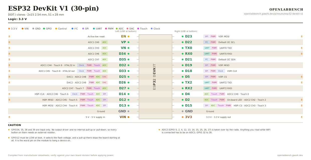
Fig. 1. ESP32 DevKit V1 (30-pin), 2x15 2.54 mm, 51 x 28 mm. Hover or tap a signal to light up every pin that carries it.
2.Caution
- GPIO34, 35, 36 and 39 are input only. No output driver and no internal pull-up or pull-down, so every button on them needs an external resistor.
- ADC2 (GPIO 0, 2, 4, 12, 13, 14, 15, 25, 26, 27) is taken over by the radio. Anything you read while WiFi is connected has to be on ADC1: GPIO 32 to 39.
- GPIO12 must be LOW at boot. It selects the flash voltage, and a pull-up there stops the board starting at all. It is the worst pin on the module to hang a device on.
- Other strapping pins: GPIO0 low enters flash mode (the BOOT button), GPIO2 must be low or floating, GPIO5 and GPIO15 are pulled high at boot and emit a PWM burst as they do.
- GPIO6 to GPIO11 wire to the SPI flash inside the module. They are not on the 30-pin header, and the 38-pin version that does expose them should not be used.
- Any output-capable pin can do PWM: the LEDC block has 16 channels and routes to any GPIO, so the usual PWM pin lists do not apply.
- VIN takes 5 V. The onboard regulator handles about 600 mA, and the radio pulls 250 mA spikes, so a thin USB cable shows up as random reboots.
3.Register configuration
Turning a pin on the diagram into a configured pin.
Drive a pin and read one
ESP-IDF v5
#include "driver/gpio.h"

gpio_reset_pin(GPIO_NUM_2);    /* clears any leftover mux setting */
gpio_set_direction(GPIO_NUM_2, GPIO_MODE_OUTPUT);
gpio_set_level(GPIO_NUM_2, 1);

gpio_config_t in = {
    .pin_bit_mask = 1ULL << GPIO_NUM_4,
    .mode         = GPIO_MODE_INPUT,
    .pull_up_en   = GPIO_PULLUP_ENABLE,
    .intr_type    = GPIO_INTR_NEGEDGE,
};
gpio_config(&in);
pin_bit_mask is 64-bit. Writing 1 << GPIO_NUM_34 instead of 1ULL << overflows a 32-bit int and silently configures nothing.
4.Full pin reference
Every pin, alias and mapping. This is the table that prints.
Table 1. Pin assignments.
| Pin | Name | Also called | Functions | Notes |
|---|---|---|---|---|
| - | EN | RST, CHIP_PU | Active-low reset | Pulled high on board. A 100 nF cap to GND here fixes boards that will not auto-reset into the bootloader. |
| - | VPADC | GPIO36, SENSOR_VP, ADC1_CH0 | ADC1 CH0 | Input only. No pull-up or pull-down. |
| - | VNADC | GPIO39, SENSOR_VN, ADC1_CH3 | ADC1 CH3 | Input only. No pull-up or pull-down. |
| - | D34ADC | GPIO34, ADC1_CH6 | ADC1 CH6 | Input only. No pull-up or pull-down. |
| - | D35ADC | GPIO35, ADC1_CH7 | ADC1 CH7 | Input only. No pull-up or pull-down. |
| - | D32ADCTouchPWMClock | GPIO32, ADC1_CH4, TOUCH9 | ADC1 CH4, Touch 9, XTAL32 in | Safe general-purpose pin, and its ADC keeps working with WiFi on. |
| - | D33ADCTouchPWMClock | GPIO33, ADC1_CH5, TOUCH8 | ADC1 CH5, Touch 8, XTAL32 out | Safe general-purpose pin, ADC1 so WiFi-safe. |
| - | D25DACADCPWM | GPIO25, DAC1, ADC2_CH8 | DAC1, ADC2 CH8 | One of only two true analog outputs, 8-bit. |
| - | D26DACADCPWM | GPIO26, DAC2, ADC2_CH9 | DAC2, ADC2 CH9 | The other 8-bit DAC. |
| - | D27ADCTouchPWM | GPIO27, ADC2_CH7, TOUCH7 | ADC2 CH7, Touch 7 | |
| - | D14SPIADCTouchPWMClock | GPIO14, HSPI_CLK, ADC2_CH6, TOUCH6 | HSPI CLK, ADC2 CH6, Touch 6 | Outputs a PWM burst at boot. |
| - | D12SPIADCTouchPWM | GPIO12, HSPI_MISO, ADC2_CH5, TOUCH5 | HSPI MISO, ADC2 CH5, Touch 5 | Strapping pin, must be LOW at boot. A pull-up here selects 1.8 V flash and the board will not start. |
| - | D13SPIADCTouchPWM | GPIO13, HSPI_MOSI, ADC2_CH4, TOUCH4 | HSPI MOSI, ADC2 CH4, Touch 4 | |
| - | GND | - | Ground | |
| - | VIN5 V | - | 5 V supply in | Same net as USB 5 V, upstream of the 3V3 regulator. |
| - | D23SPIPWM | GPIO23, VSPI_MOSI | VSPI MOSI | Default MOSI in the Arduino core. |
| - | D22I²CPWM | GPIO22, SCL | Default I2C SCL | |
| - | TX0UARTPWM | GPIO1, U0TXD | UART0 TXD | Shared with the USB bridge and the boot log. |
| - | RX0UARTPWM | GPIO3, U0RXD | UART0 RXD | Shared with the USB bridge. High at boot. |
| - | D21I²CPWM | GPIO21, SDA | Default I2C SDA | |
| - | D19SPIPWM | GPIO19, VSPI_MISO | VSPI MISO | |
| - | D18SPIPWMClock | GPIO18, VSPI_CLK, SCK | VSPI CLK | |
| - | D5SPIPWM | GPIO5, VSPI_CS, SS | VSPI CS | Strapping pin: pulled high at boot and emits a PWM burst as it starts. |
| - | TX2UARTPWM | GPIO17, U2TXD | UART2 TXD | Free second serial port. Nothing else uses it. |
| - | RX2UARTPWM | GPIO16, U2RXD | UART2 RXD | |
| - | D4ADCTouchPWM | GPIO4, ADC2_CH0, TOUCH0 | ADC2 CH0, Touch 0 | |
| - | D2ADCTouchPWM | GPIO2, ADC2_CH2, TOUCH2, LED_BUILTIN | On-board LED, ADC2 CH2, Touch 2 | Strapping pin: must be low or floating at boot. Also the blue on-board LED. |
| - | D15SPIADCTouchPWM | GPIO15, HSPI_CS, ADC2_CH3, TOUCH3 | HSPI CS, ADC2 CH3, Touch 3 | Strapping pin: high at boot. Pull it low to silence the boot log on TX0. |
| - | GND | - | Ground | |
| - | 3V33.3 V | - | 3.3 V supply out | About 600 mA from the on-board regulator, less the radio's draw. |
Primary sources
Found a wrong pin? The whole board is one file, data/boards/esp32-devkit-v1.json.